
반도체 패키징
첨단 집적을 위한 글래스 인터포저 및 코어 웨이퍼 기술
YEKGLASS는 2.5D/3D IC, FOWLP, SiP를 비롯한 차세대 반도체 집적 기술에 최적화된 맞춤형 글래스 웨이퍼를 공급합니다.
글래스 플랫폼 특유의 높은 정밀도와 뛰어난 전기적·열적 신뢰성으로 패키징의 모든 레이어를 지원하며,
패널 레벨 패키징부터 글래스 코어 기판, 저CTE 기판에 이르기까지 주요 반도체 패키징 규격을 아우르는 솔루션을 제공합니다.
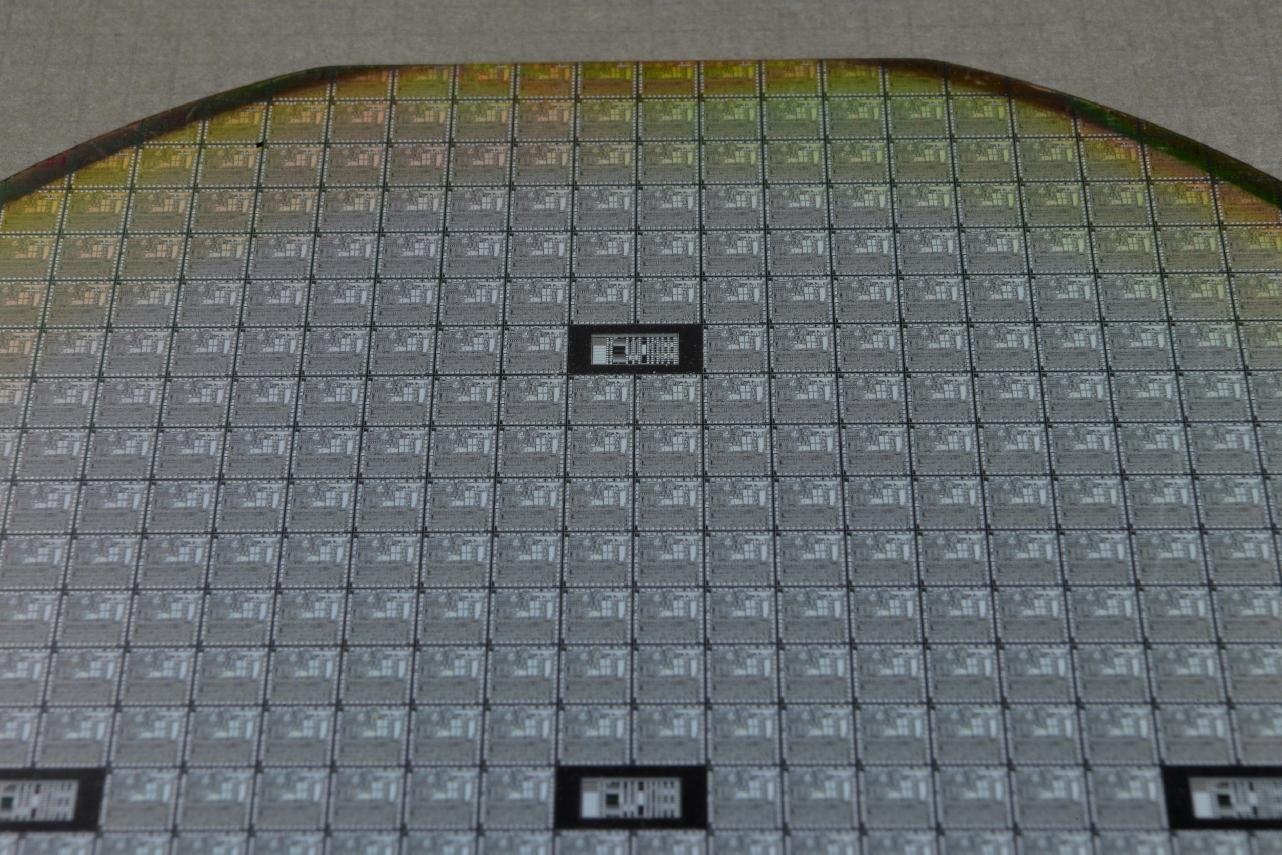
반도체 패키징을 혁신을 이끄는 초정밀 글래스 기술
YEKGLASS는 첨단 반도체 패키징을 위한 초정밀 가공 글래스 웨이퍼를 공급합니다.
다층 적층, 모듈형 조립, 고밀도 RDL 빌드업 공정 솔루션과, 독자적 몰딩 기술을 통한 금속 핀 임베딩(Embedding)을
구현합니다. 초평탄·저CTE 글래스 코어 기판은 패키징 전 공정에 걸쳐 탁월한 치수 안정성을 제공할 수 있습니다.
2.5D & 3D IC 패키징
TGV 및 전도성 엘리먼트가 내장된 글래스 웨이퍼를 통해 소형 모듈의 수직 집적, 고속 신호 전달, 효과적인 열 관리를 구현합니다.
팬아웃 웨이퍼 레벨 패키징
초평탄 코어 글래스 기판이 재배선층(RDL)의 변형을 방지하고 정밀도를 유지해, 박형(Low-profile) 및 고비용 효율 패키지의 공정 정렬 신뢰성을 대폭 향상시킵니다.
시스템 인 패키지 (SiP)
캐비티 구조의 글래스 웨이퍼는 완벽히 기밀 실링된 글래스 아키텍처 내부에서 RF, 센서, 메모리 등 다양한 기능성 모듈의 다기능 집적을 지원합니다.
RF, 광학 & 파워 모
글래스 고유의 우수한 유전 안정성과 기밀 특성을 바탕으로 가혹한 작동 환경에서도 고주파 및 고전압 부품을 안정적으로 보호합니다.
글래스 패키징의 주요 특성 및 장점
YEKGLASS는 수십 년간 축적된 글래스 제조 전담 노하우를 바탕으로 반도체 패키징 솔루션의 성능과 신뢰성을 한 단계 끌어올립니다.
향상된 수율과 검증된 신뢰성을 바탕으로, 고객의 차세대 반도체 소자 설계를 위한 확실하고 효율적인 경로를 제시합니다.
초정밀 미세 가공

YEKGLASS는 독자적인 몰딩 및 에칭 기술을 기반으로 비아, 캐비티, 채널, 엣지 정의 구조 등 미세 패턴을 30µm 이하의 정밀도로 구현합니다. 엣지 치핑을 최소화하여 복잡한 3차원 직접을 가능하게 하며, MEMS, 센서, 고밀도 IC 패키징에 가장 이상적인 솔루션을 제공합니다.
열적 & 기계적 안정성

기존의 비아 드릴링 및 전기도금 공정 대신, 글래스 웨이퍼 몰딩 단계에서 전도성 금속 핀을 직접 내장하는 원스톱 공정을 적용합니다. 이를 통해 기계적 응력을 극대화하여 줄이고 미세 균열을 원천 차단하며, 금속 핀과 글래스 간의 강력한 접합 신뢰성을 보장합니다.
유전 특성

유리는 본래 유전율과 손실계수가 낮아 고주파 영역에서도 우수한 전기 절연성과 최적의 신호 손실 방지 성능을 발휘합니다. 이러한 특성은 신호 무결성이 핵심인 RF 모듈, 초고속 데이터 전송선, 광통신 부품에 최적화되어 있습니다.
기밀성 & 신뢰성

글래스 기판 고유의 수분·가스·화학물질 차단 성능을 바탕으로 완벽한 기밀 실링을 구현하여 가혹한 외부 환경으로부터 내부 소자를 안전하게 보호합니다. 이는 항공우주, 의료, 고전압 전자기기 등 치명적인 오류가 허용되지 않는 한 미션 크리티컬 시스템에서 필수적인 신뢰성을 제공합니다.
YEKGLASS 글래스 패키징 기술의 핵심 경쟁력
YEKGLASS는 독자적인 몰딩 기술로 TGV, 캐비티, 도전성 핀을 단일 공정(Single-step)에서 동시에 구현합니다.
복잡한 기계적 드릴링과 플레이팅 공정을 근본적으로 단축함으로써 공정 수율 극대화와 생산 단가 절감을 이뤄냈으며,
기계적 내구성 및 전기적 특성의 산사(Variation)를 최소화하여 패키징 전체의 기술 신뢰성을 한 단계 끌어올렸습니다.
| 기존 패키징 공정 | YEK 단일 몰딩 솔루션 |
|---|---|
| 비아 드릴링 및 도금 공정 | 글래스 내 금속 핀 직접 몰딩 |
| 패키징 레이어 간 높은 CTE 불일치 | 저 CTE 글래스로 열 응력 없는 접합 구현 |
| 유기 코어 소재의 시간에 따른 열화 | 글래스 소재의 완벽한 기밀성 및 장기 신뢰성 |
| 제한된 설계 유연성 | 맞춤형 캐비티, 비아 및 웨이퍼 스펙 대응 가능 |

YEKGLASS와 함께 차세대 IC 패키징의 기술적 혁신을 만나보세요.
글래스 인터포저, 코어 기판부터 공정 맞춤형 본딩 지원까지, 공정 요구사항에 부합하는 최적의 기술 지원을 제공합니다.
IC 패키징 최적화를 위한 맞춤 솔루션
첨단 반도체 패키징을 위한 글래스 기반 플랫폼
YEKGLASS는 다양한 패키징 공정에 대응하여 조정 가능한 맞춤 글래스 솔루션을 공급하고 있습니다.
첨단 반도체 집적을 구현하는 YEK의 핵심 기술 플랫폼을 확인하세요.
유리 조성 기반의 저온 실링 소재로, 글래스·금속·세라믹 부품 간의 접합에 최적화되어 있습니다. 파우더 또는 페이스트 형태로 공급되며, 최적화된 공정 조건에서 우수한 접착력, 열적 내구성, 기밀 실링을 구현합니다. 초소형 소자 및 패키징 유닛의 보호 실링 형성에 적합합니다.

글래스 프릿 & 페이스트
TGV, 맞춤형 캐비티, 선택적 전도성 피쳐 통합을 지원하는 정밀 가공 글라스 웨이퍼입니다. YEKGLASS의 독자적인 글래스 몰딩 기술을 활용하여 소형 전자 모듈의 다층 집적 및 신호 라우팅에 최적화된 플랫폼 웨이퍼를 제공합니다. 뛰어난 정렬 정밀도, 설계 유연성, 공정 호환성을 갖추고 있습니다.
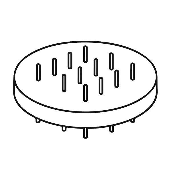
정밀미세가공 글래스 웨이퍼
소자 캡슐화 및 구조적 지지를 위해 맞춤형 캐비티 구조, 단차 프로파일,
측벽 성형 기술을 적용한 글래스 웨이퍼입니다. 우수한 평탄도와 정밀한 치수 제어력을 바탕으로 웨이퍼 레벨 통합, 정밀 소자 하우징, 실링 응용 분양에 적합합니다. 광학 투명성, 표면 연마, 코팅 등 고객 요구에 맞춘 다양한 옵션을 제공합니다.

글래스 웨이퍼 패키징
