
Semiconductor Packaging
Glass Interposer & Core Wafer Technologies for Advanced Integration
YEKGLASS provides application specific glass wafer solutions for next generation semiconductor integration, including 2.5D/3D IC, FOWLP, and SiP.
Our glass based platforms deliver precision, electrical connectivity, and thermal reliability for every packaging layer.
Our solutions address panel level packaging (PLP), glass core substrate, and low CTE glass substrate requirements across leading semiconductor packaging architectures.
Where Glass Makes a Difference in Packaging
YEKGLASS provides precision-engineered glass wafers for advanced semiconductor packaging.
Our solutions support multi-layer integration, modular assemblies, and high-density RDL build-up.
Proprietary molding technology enables metal pin embedding, while ultra-flat, low CTE core glass ensures dimensional stability throughout the packaging process.
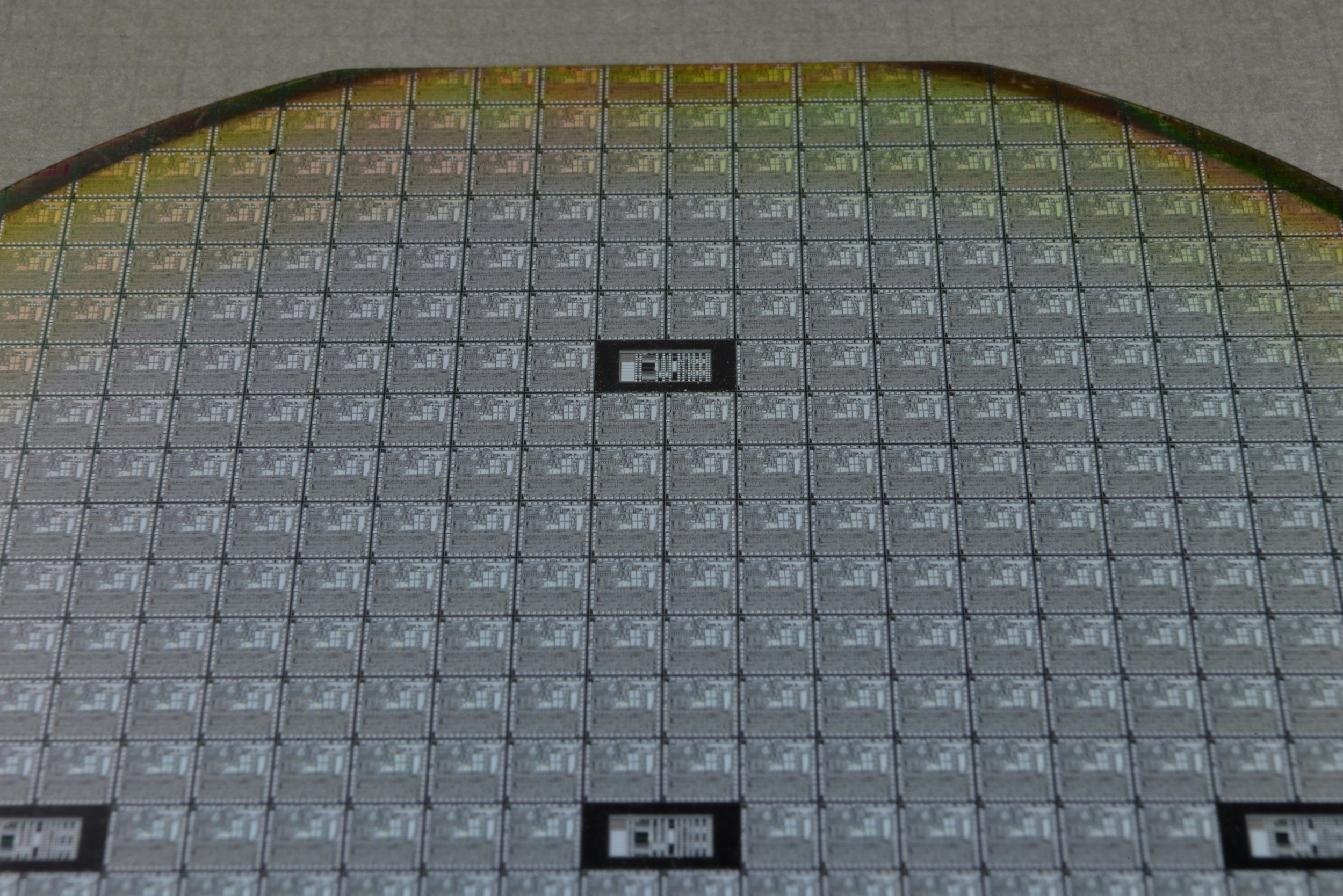
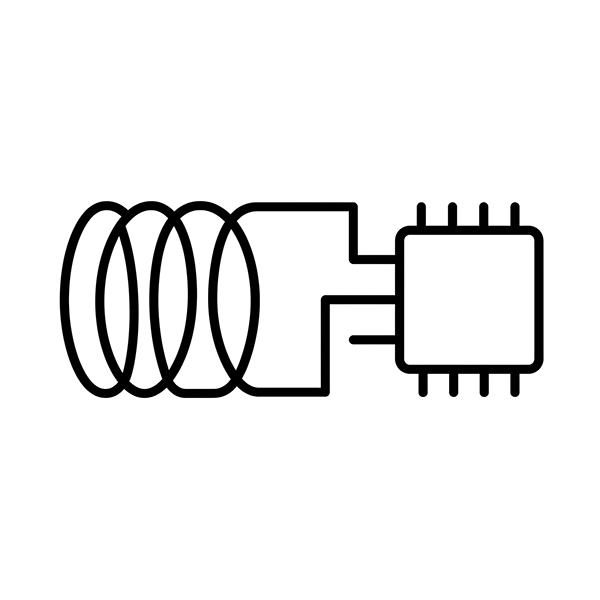
2.5D & 3D IC Packages
Glass wafers featuring TGV and embedded conductive elements facilitate vertical integration, signal transmission, and thermal management in compact electronic assemblies.
Fan-Out Wafer-Level Packaging
Ultra-flat core glass substrates stabilize redistribution layers and improve process alignment in low profile, cost effective packages.
System-in-Package
Cavity-structured glass wafers support multi-functional module integration RF, sensor, memory within hermetically sealed glass architectures.
RF, Optical & Power Modules
Glass's dielectric stability and hermetic properties protect high frequency and high voltage components in demanding operating environments.
Key Features & Advantages of Glass-Based Packaging
YEKGLASS applies decades of specialized glass manufacturing expertise to enhance the performance and reliability of semiconductor packaging solutions.
Our solutions deliver higher yields, better reliability, and a streamlined path toward next generation device designs.
Ultra-Precise Structuring

YEKGLASS uses proprietary glass molding and etching technologies to create micro scale features such as vias, cavities, channels, and edge defined structures with sub 30 μm accuracy. This precision allows complex integration with minimal edge chipping, making it ideal for MEMS, sensors, and high density IC packaging.
Thermal & Mechanical Stability

Instead of drilling vias and performing electroplating, we embed conductive metal pins during the glass wafer molding process. This single step approach minimizes mechanical stress, prevents microcracks, and ensures consistent pin to glass adhesion.
Dielectric Performance

Glass exhibits inherently low dielectric constant and low loss tangent, providing excellent electrical insulation and minimal signal interference at high frequencies. This makes it a superior material for RF modules, high speed signal lines, and optical communications where signal integrity is critical.
Hermetic & Reliable

With natural resistance to moisture, gas, and chemicals, glass substrates ensure true hermetic sealing protecting internal components from environmental damage. This reliability is essential in mission critical systems such as aerospace, medical, and high voltage electronics, where failure is not an option.
Why YEKGLASS
Our proprietary glass molding process forms TGV, cavities, and metal pins simultaneously in a single step.
This eliminates conventional drilling and electroplating, reducing process complexity and improving yield.
The result is better mechanical integrity and more consistent electrical performance across the packaging layer.
| Traditional Packaging | YEKGLASS Solution |
|---|---|
| Via drilling + plating needed | Direct metal pin molding in glass |
| High CTE mismatch with packaging layers | Low CTE glass ensures stress-free bonding |
| Organic core materials degrade over time | Glass provides hermetic, long-term reliability |
| Limited design flexibility | Custom cavities, vias, and wafer formats available |

Collaborate with YEKGLASS to engineer the next evolution in IC packaging.
Whether you need glass interposers, core substrates, or application-specific bonding support, our global team is ready to help you scale with confidence.
Discuss Your Packaging Requirements With Us
Glass-Based Platforms for Advanced Semiconductor Packaging
YEKGLASS offers reliable and customizable glass components engineered to support a wide range of packaging processes.
Discover the core platforms behind advanced semiconductor integration.
Low-temperature sealing materials based on glass compositions, suitable for bonding between glass, metal, or ceramic components. Available in powder or paste form, our materials provide strong adhesion, thermal durability, and hermetic sealing under optimized processing conditions. Ideal for forming protective seals in miniaturized devices and packaging units.

Glass Frit & Paste
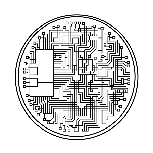
Precision-processed glass wafers with through holes, custom cavities, and optional conductive feature integration. Using our proprietary glass forming technology, we provide platform wafers suitable for multi layer integration and signal routing in compact electronic modules. These wafers support high alignment accuracy, design flexibility, and process compatibility.
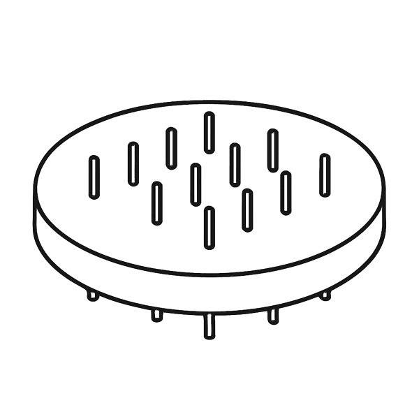
Micro Structured Glass Wafer
Glass wafers featuring custom cavity structures, stepped profiles, and sidewall shaping for device encapsulation and structural support. Their flatness and high dimensional control make them suitable for wafer level integration, sensitive device housing, and sealing applications.
Options such as optical transparency, surface polishing, and coating are available for diverse needs.

Packaging Glass Wafers

Looking for Precision and Reliability in Glass Packaging?
Tell us about your project goals or technical challenges. Let’s build it—exactly the way you need.